What you'll learn
01
Stackup and materials
How stackup and material choices set your loss budget before routing starts.
02
Vias and breakout
What via stubs, back-drilling and breakout cost in return loss and crosstalk margin, with numbers from real boards.
03
Discontinuities
Where BGA pads, connector, and AC coupling capacitor footprints create discontinuities, and how to reduce them.
04
The road to 224G and beyond
Why 112G reference channels run short of bandwidth for 224G PAM4.
Key details
- Date: Thursday, November 5, 2026
- Time: 1:00 PM ET / 10:00 AM PT
- Duration: 30 minutes (20-minute presentation followed by live Q&A)
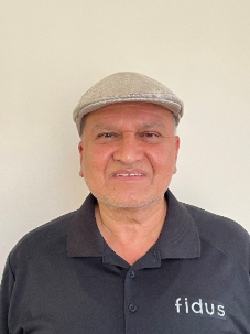
- Speaker: Dr. Syed A. Bokhari, Signal Integrity and EMC Architect, Fidus
Can't make it live? Register anyway and we'll send you the recording.
About this webinar
At 112G PAM4, and beyond, most of your channel margin is won or lost in the printed circuit board itself. Join Fidus Signal Integrity Architect Dr. Syed Bokhari for a tech talk that walks through a real 112G channel budget, line by line, and shows what each layout decision costs.
Drawing on Fidus printed circuit board and package work rather than textbook examples, Syed will cover stackup and material choices, via design and back-drilling, AC capacitor, and connector footprints and reference-plane apertures. He will close with what changes are needed as the industry moves to 224G, and why boards being laid out today are already running short of bandwidth.